2.11 Sensors: photosites, CCD vs CMOS⧉
We have been treating the pixel as an abstraction: a number that integrates incoming light over a little patch of the image. It is time to look at the thing that actually produces that number, the image sensor, because how it is built, and above all how it is read, quietly decides a great deal of what a camera can and cannot do. The previous chapter owned three axes of the pixel integral (the aperture, the pixel's area, and wavelength); this chapter owns the fourth, time, and the mechanism that opens and closes it: the shutter.
2.11.1 The photoelectric effect⧉
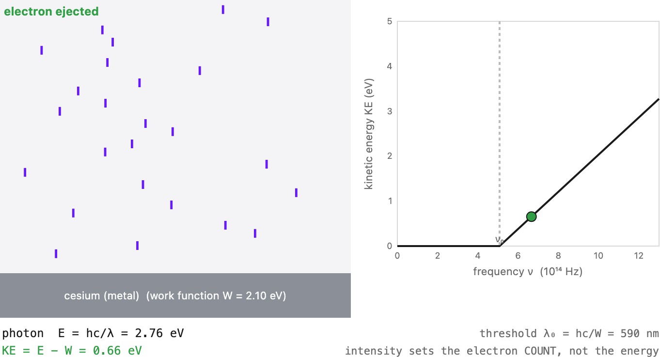
Before a sensor can count light, something physical has to turn light into an electrical signal, and that something is the photoelectric effect: light striking matter frees electrons. Heinrich Hertz stumbled on it in 1887, and it flatly refused to fit the wave theory of light. The puzzle was sharp. Shine a brighter light and, classically, you should knock electrons loose with more energy, and any color should work so long as you make it intense enough. Experiment said the opposite. Below a certain threshold frequency no electrons come out at all, however intense the beam, and above that threshold the energy of each ejected electron depends only on the light's frequency (its color), not on its brightness. Turning up the intensity frees more electrons but gives no single one of them any more energy.
The photon explanation of the photoelectric effect was only one of four papers Albert Einstein published in 1905, his annus mirabilis (miracle year), while he was a junior clerk in the Swiss patent office with no university post. In a few months he (1) quantized light into photons, $E = h\nu$, to explain the photoelectric effect, the paper the 1921 Nobel Prize would cite; (2) explained Brownian motion as the jostling of molecules, giving decisive evidence that atoms are real; (3) introduced special relativity, dissolving absolute time and space; and (4) derived $E = mc^2$. Any one of these would have made a career; together they remade physics in a single year. It is worth remembering, whenever a sensor counts photons, that the photon itself was born in that year, and that Einstein's Nobel went not to relativity but to this quiet fact about light and electrons that every digital camera now runs on.
Einstein resolved this in 1905, the work for which he was awarded the Nobel Prize, by taking light to be quantized into particles (photons), each carrying an energy fixed by its frequency,
with $h$ Planck's constant, so shorter wavelengths carry more energy per photon. An electron is held in the material by a binding energy $W$ (a metal's work function, or, in a semiconductor, the band gap $E_g$ that separates bound from mobile electrons). A single photon can free a single electron only if it carries enough energy to pay that price, and the surplus becomes the freed electron's kinetic energy,
This is a threshold, not a dimmer. A red photon that falls short of $W$ frees nothing no matter how many of them arrive, while one blue photon above the threshold does the job. Brightness is just the number of photons per second, so it sets the number of freed electrons, not the energy of each. That is the whole quantum story of light detection in one line, and Figure 2.11.1 lets you dial the wavelength, the material, and the intensity and watch it play out.
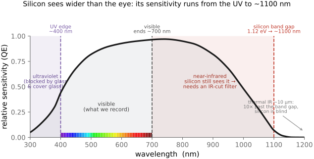
A digital sensor runs on the internal version of the effect. In silicon a photon with energy above the band gap ($E_g \approx 1.12$ eV, a wavelength near $1100$ nm) is absorbed and frees an electron-hole pair inside the crystal, where it can be collected, rather than ejected into vacuum as in the classic metal-cathode experiment and in photomultiplier tubes. Every visible photon, from red at about $1.8$ eV to violet at about $3.1$ eV, clears silicon's gap comfortably, so each one that is absorbed contributes close to one electron to the well. That one-photon-one-electron bookkeeping is exactly why a photosite is a linear counter of light, the property the next section is built on. It also pins down two practical facts we return to: silicon keeps responding out to about $1100$ nm, so a color camera needs an infrared-cut filter in front of the sensor to stop invisible near-infrared from polluting the image, and no detector catches every photon that lands, so the fraction it does convert to signal is its quantum efficiency.
2.11.2 Photon to number: the photosite⧉
A digital sensor is a two-dimensional array of photosites, one per pixel. Each photosite is a small potential well that counts photons: arriving light frees electrons, the well accumulates that charge, and at the end of the exposure the charge is converted to a voltage and then, by an analog-to-digital converter (ADC), to a number. Because the well literally counts arrivals, the number it reports is, to good approximation, linear in the amount of light that fell on it. That linearity is not a minor technical detail: it is what lets us treat a raw image as a calibrated radiometric measurement, and it is the foundation that makes HDR merging, deblurring, and depth estimation meaningful later in the book.
A photosite is at heart a photon counter: each absorbed photon frees a charge carrier — an electron, or equivalently a hole (a missing electron) — and the well accumulates them in direct proportion to the light that arrives. So the raw signal is linear in scene radiance, before any gamma or tone curve. This linearity is not a detail; it is what makes raw arithmetic trustworthy: HDR merging adds exposures, white balance is a per-channel multiply, flat-field correction is a divide, and all three are valid only because the numbers are proportional to light. Display encoding (gamma) deliberately hides this linearity for the eye — so computation should undo it and work in linear light.
It is worth separating two revolutions that are often conflated. The first was electronic imaging: turning light into an analog electrical signal (the era of the CCD and analog video). The second, the one computational photography lives on, was digital: putting an ADC in the path so the signal becomes numbers we can compute on. A sensor that captures light electronically but never digitizes it is a television camera, not a computer's eye.
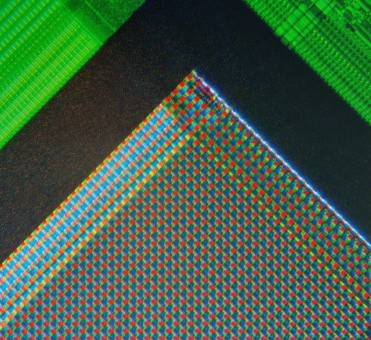
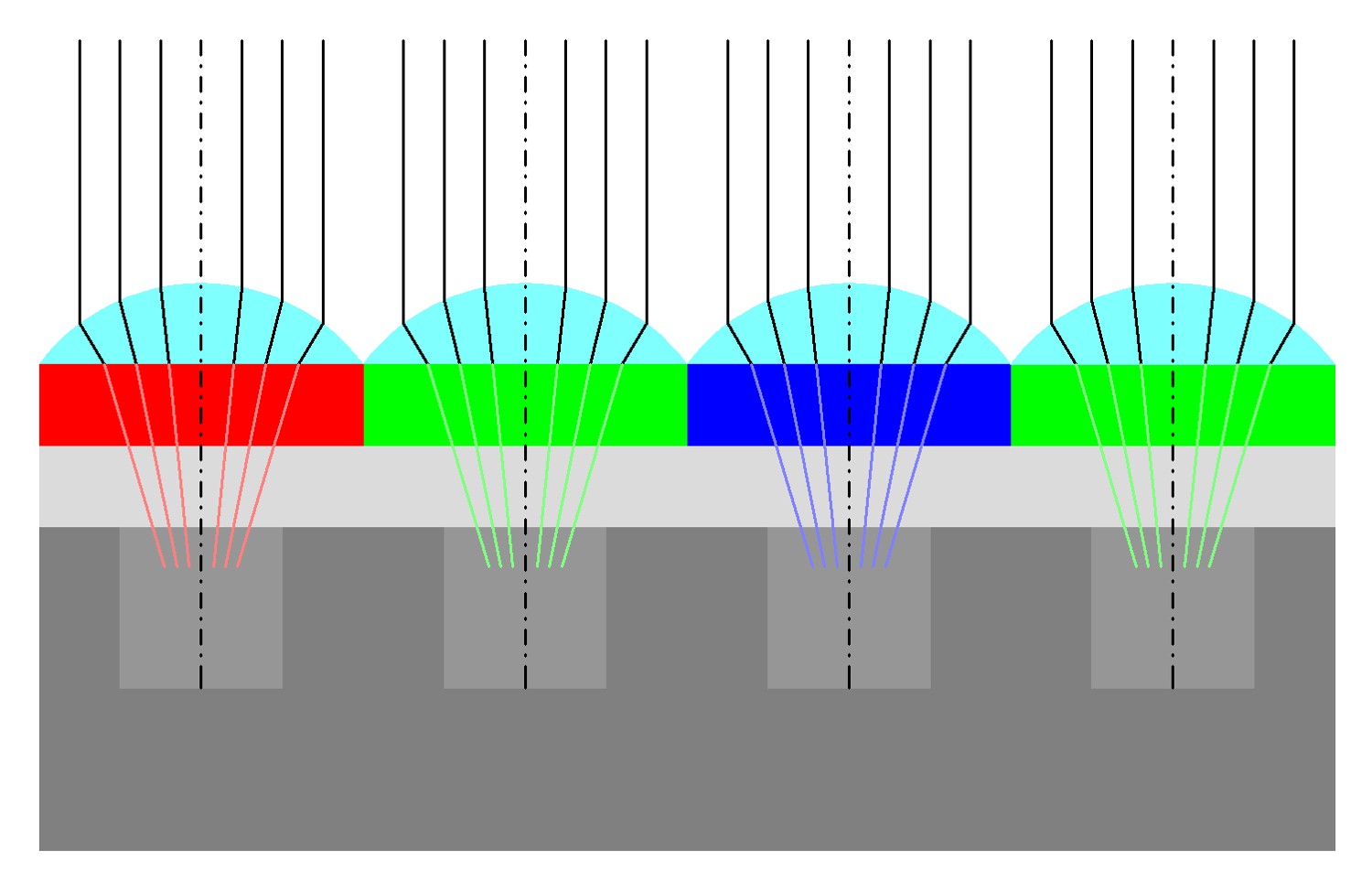
Above each photosite sits a microlens that funnels light onto the light-sensitive area — necessary because wiring occupies part of each pixel, so the fill factor is less than 100%. Under the microlens sits a color filter, and the mosaic of red, green, and blue filters (the Bayer pattern) is why color must be reconstructed by demosaicking (a later chapter). Finally, the map from scene radiance to the rendered pixel value is the camera response curve: raw is roughly linear, while a JPEG has a non-linear curve (gamma plus a tone curve) baked in — recovering that curve is exactly the problem HDR has to solve.
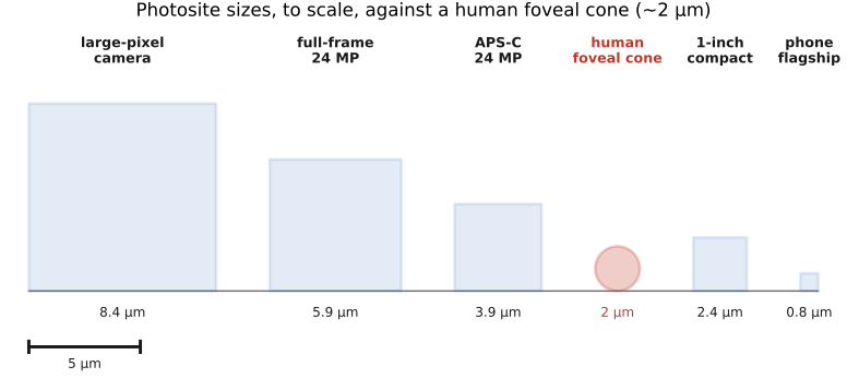
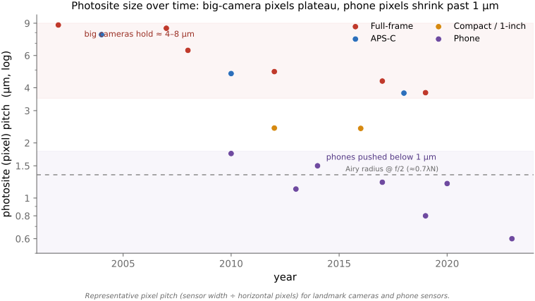
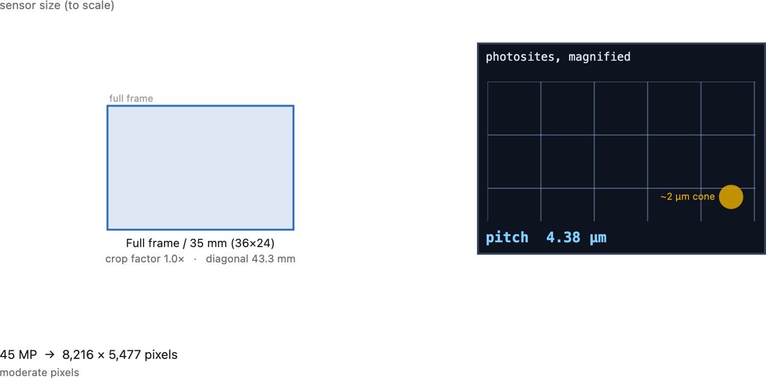
How big is a photosite, really? Pixel sizes span more than a factor of ten across cameras, and the range maps directly onto the sensor-size story below. A flagship phone crams its pixels down to about $0.7$–$1.0\,\mu\text{m}$; a 1-inch compact sits near $2.4\,\mu\text{m}$; APS-C runs $3.5$–$4\,\mu\text{m}$; a full-frame sensor is $4$–$6\,\mu\text{m}$; and the largest-pixel cameras (low-resolution full-frame bodies, astronomy and scientific sensors) reach $8\,\mu\text{m}$ and beyond. The telling comparison is biological: a foveal cone is about $2\,\mu\text{m}$ across (the eye's photoreceptors), so a big camera pixel is several cones wide, while a modern phone pixel has shrunk below the size of a single cone (Figure 2.11.4). Size is destiny here because a bigger well catches more photons and so carries less shot noise for the same scene, which is the whole reason larger sensors look cleaner (→ The impact of sensor size, below). The phone's tiny wells force it to make up the deficit computationally, with burst capture and denoising rather than glass and silicon.
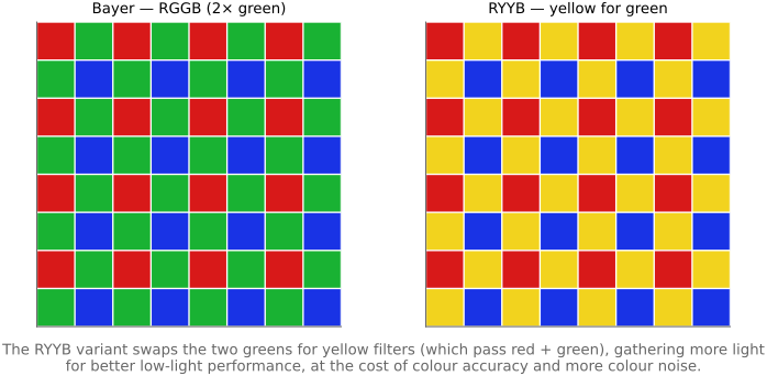
Strip away the color filter and a sensor is monochrome at the pixel: each photosite reports a single number, the count of photons it caught — not a color. The three (or more) values that color needs must therefore be multiplexed along some other axis: over space (a color-filter array such as Bayer, paying with resolution and a demosaicking step), over time (sequential color filters, paying with motion robustness — the old color-wheel and many scientific cameras), across multiple sensors (a beam-splitter prism feeding three chips, the 3-CCD video camera, paying with bulk and cost), or over depth (wavelength-dependent absorption in stacked photodiodes, the Foveon, paying with noise). Every color camera is a choice of which axis to spend. The same constraint shapes the eye, whose three cone types sample color over space at the retina (L2.10, L2.13).
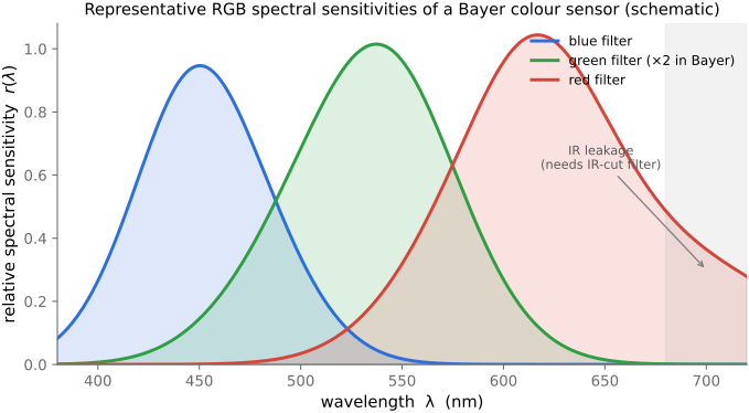
2.11.3 Spectral sensitivity: matching the eye, catching photons, and white balance⧉
The exact shape of those three curves, the sensor's spectral sensitivity, is one of the camera's most constrained choices, because it is pulled in three directions at once that cannot all be satisfied.
- Fidelity to human vision. For a camera to record the color a human would see, its three curves should be a fixed linear combination of the eye's cone fundamentals (equivalently, of the CIE color-matching functions) — the Luther–Ives condition. A sensor that met it could be mapped to human color by a single $3\times3$ matrix with no error. Every real sensor violates it, because silicon-plus-dye curves are simply the wrong shape, and the penalty is a metameric error no color matrix can remove: two spectra that look identical to the eye read as different RGB, and two that look different can read the same. The color-correction matrix in the ISP is a least-squares compromise — right on average, wrong on the hard cases (saturated reds, narrow-band LEDs, foliage).
- Quantum efficiency and noise. Quantum efficiency — the fraction of arriving photons actually counted — rewards broad, overlapping passbands: the wider each filter, the more photons reach the well and the higher the SNR. But broad overlap is exactly what destroys color separation, because strongly correlated channels must be differenced to pull color out, and differencing amplifies noise (the same reason the eye's overlapping L and M cones force an opponent stage, L2.14). Narrow, well-separated filters give clean color but throw photons away and read noisier. The green-doubled Bayer is one point on this curve — spend photons and resolution where the eye cares most (luminance), economize on chroma.
- White balance across illuminants. Because each channel integrates illuminant × reflectance × sensitivity, changing the light changes the raw RGB of a fixed object. Undoing that — white balance, ideally a per-channel gain (von Kries) — is only exact when the sensitivities behave like the cones; the further they stray, the more a single diagonal (or even $3\times3$) fails to hold colors constant as the light shifts from daylight to tungsten to a spiky fluorescent. Good spectral design makes white balance more reliable across illuminants (→ auto white balance).
These three pull against each other: the curves that best match the eye are broad and overlapping (bad for separation), the curves that separate color cleanly are narrow (bad for QE and for matching the eye), and keeping white balance stable across odd illuminants wants yet another shape. Every color sensor is a negotiated settlement among them (Figure 2.11.7).
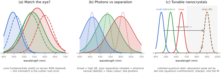
Nanocrystals — spectral sensitivity as a design parameter. In a conventional sensor, dye filters and silicon absorption largely determine the spectral curves. Colloidal quantum dots (semiconductor nanocrystals, a few nanometres across) change that: because a dot's bandgap — and so the wavelength it absorbs — is set by its size through quantum confinement, a solution-processed quantum-dot layer has a tunable, often sharper spectral response that can be dialled in per channel and pushed into the short-wave infrared or ultraviolet that silicon handles poorly. Laid as a thin film on top of the read-out circuitry, such a layer also absorbs strongly in far less depth than silicon — help exactly where it hurts most, the sub-micron pixels whose shrinking well we meet next. Quantum-dot and other tunable-absorber sensors are still maturing, but they point to a future where the settlement above is no longer fixed by materials chemistry but engineered. This is analogous to the nano-prism color router below, which attacks the photon-efficiency leg by routing color instead of absorbing it. Nanocrystals return in the colour chapter as a hybrid of spatial multiplexing and the prism idea.
How big is a photosite? The single most consequential number about a sensor is the pixel pitch — the physical size of one photosite — because it sets how many photons a pixel can gather (and how many electrons its well can hold). The range across cameras is enormous. A full-frame camera's photosites are typically 4–8 µm across; an APS-C body's are similar; a 1-inch compact's around 2.4 µm; and a modern phone's are around 0.6–1.4 µm — roughly five to ten times smaller in each dimension, so 25–100× smaller in area and in light gathered per pixel. And the trends diverge (Figure 2.11.8): big-camera pixels have hovered around 4–8 µm for two decades (more resolution was bought mostly by bigger sensors, not much smaller pixels), while phone pixels have been driven relentlessly down, now well below a micron. This continued shrinking is why phones must bin pixels in low light (the quad-Bayer trick below), and why it runs into hard physical floors: a sub-micron pixel approaches the diffraction-limited spot size of the lens (the Airy disk is already ~1.3 µm wide at $f$/2), so further shrinking buys megapixels the optics cannot actually resolve, and the tiny full-well capacity caps dynamic range. The impact of pixel and sensor size on light gathering, depth of field, and noise gets its own section below.
2.11.4 Beyond the visible spectrum: near-infrared, thermal, and ultraviolet⧉
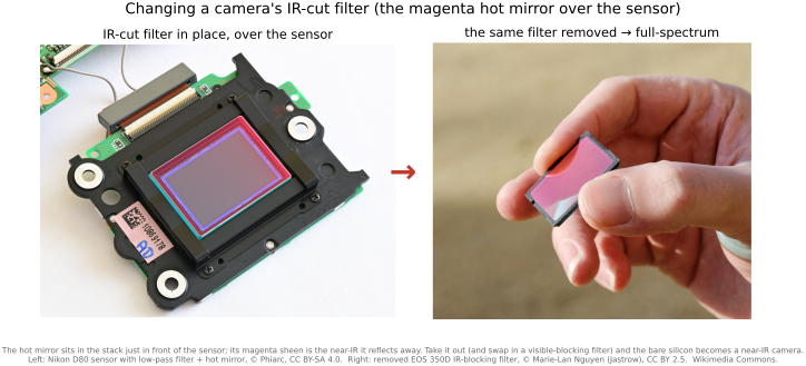
Silicon does not stop at the red end of the visible spectrum. Its band gap sits near $1100$ nm, so a photosite keeps counting photons well into the near-infrared, a band the eye cannot see at all. That extra reach is normally a nuisance: uncontrolled near-IR would haze color images with light the eye never registers, so every color camera carries an infrared-cut filter (a "hot mirror") in front of the sensor to throw it away. The spectral-sensitivity curves above already show this — their long-wavelength tails are cut not by the silicon but by that filter. Silicon's own reach is wider than the eye's at both ends (Figure 2.11.9).
Remove the hot mirror (Figure 2.11.10) and put in its place a filter that blocks visible light instead, and the very same sensor becomes a near-infrared camera (Figure 2.11.11).
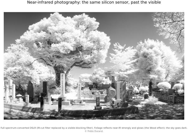
Near-infrared is not thermal infrared. This point causes endless confusion, so it is worth stating plainly. The near-infrared just discussed (roughly 700–1100 nm) is reflected light: it behaves like an invisible extension of visible color, needs an external source (the sun, or an IR LED) to illuminate the scene, and is caught by ordinary silicon. Thermal infrared is a completely different band and a completely different mechanism. Every object near room temperature glows by blackbody radiation, but its emission peaks around 10 µm (long-wave IR), roughly ten times the wavelength silicon can reach: those photons carry far less energy than silicon's band gap, so a normal sensor is stone blind to them. Detecting body heat in the dark therefore needs an entirely different detector, a microbolometer or a cooled InSb / HgCdTe array, behind special (often germanium) optics, which is why thermal cameras are their own expensive category. So "infrared camera" splits in two: a cheap modified silicon camera sees reflected near-IR (bright foliage, dark sky, and it needs light in the scene), while a thermal camera sees emitted long-wave IR (glowing warm bodies, works in total darkness) and shares almost nothing with it but the word.
A word on ultraviolet. The short-wavelength edge is the mirror image. Silicon has some genuine response below 400 nm, but two things usually block it before it reaches the photosite: ordinary glass lenses absorb UV, and the sensor's own cover glass and filters cut it. Swap in quartz or fluorite optics and a UV-pass filter and the same silicon can do reflected-ultraviolet photography, which reveals things invisible to us: sunscreen painted on skin, the nectar-guide patterns on flowers that steer pollinators, and surface detail in questioned documents and paintings. As with the infrared cut, the visible window we normally record is not a limit of the detector but a band we deliberately trim to with filters.
2.11.5 Analog-to-digital conversion⧉
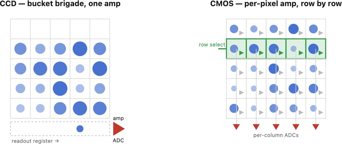
The last step of capture is the one that makes computational photography possible at all: turning each photosite's accumulated charge into a number. At the end of the exposure the charge in a well is read out as a small voltage, optionally amplified (this is where ISO / gain acts — see below), and then handed to an analog-to-digital converter (ADC) that quantizes it to an integer. Modern CMOS does this massively in parallel: a column-parallel ADC array — often one converter per column, sometimes per pixel — digitizes a whole row at once, which is exactly what makes high-resolution, high-frame-rate readout feasible.
Two numbers describe the conversion. The bit depth sets how finely the voltage range is sliced: a 12-bit raw file has 4096 levels, 14-bit has 16384, a 16-bit medium-format back more still. The subtler number is where those levels fall — because the signal is linear in light (L2.39), equal code steps are equal amounts of light, so the deep shadows are described by proportionally few codes. This is why raw is stored linearly but with generous bit depth (so even the sparse shadow codes outnumber the noise), and why display encoding later applies gamma to redistribute codes perceptually. It is also the one place where quantization — usually not the limiting factor (L2.49) — can bite, showing up as banding in a smooth gradient when there are too few bits.
The order of operations matters for noise. Analog gain (ISO) is applied to the voltage before the ADC, so raising ISO lifts the photon signal and the sensor's upstream noise together up above the converter's quantization and the downstream read noise — which is why a higher-ISO capture can be cleaner in the deep shadows than brightening a low-ISO file afterward (a dual-conversion-gain sensor, below, exploits precisely this). Past the ADC the image is just numbers, and everything the rest of this book does begins there.
2.11.6 CCD versus CMOS⧉
For decades the dominant sensor was the CCD (charge-coupled device). A CCD has no per-pixel electronics; instead it shuttles the accumulated charge across the chip in a "bucket brigade" to a single amplifier at the edge, where it is measured. This makes CCD output clean and uniform, and because the whole frame is transferred together it is naturally a global capture — but it is slow, power-hungry, and cannot put much intelligence on the chip.
The CMOS sensor, now utterly dominant, puts an amplifier — and increasingly the ADC and digital logic — at every pixel, and reads the array out row by row like memory. This is cheap, fast, and low-power, and it is what makes modern computational sensors possible: on-chip ADCs, high-frame-rate and region-of-interest readout, on-sensor HDR, phase-detect autofocus, and pixel binning. The price of reading row by row is that different rows are captured at slightly different times — the rolling shutter, which we return to below.
2.11.7 Time integration: the exposure⧉
Over the exposure time $\Delta t$, the well accumulates photons, so the pixel value is the time integral of the irradiance it receives: $\text{value} \propto \int_0^{\Delta t} E\,dt$. This is the fourth axis of the pixel integral, and it is governed by two controls — the aperture (how much light per unit time) and the exposure time — with ISO applying gain after capture. The familiar trade, exposure = irradiance × time, means halving the light and doubling the time gives the same exposure (reciprocity); digital sensors obey this far more faithfully than film, whose reciprocity failure at long exposures was a perennial nuisance.
The time integral is motion blur: anything that moves during $\Delta t$ is averaged along its path. A long exposure smears motion into light trails and silky water; a short one freezes a hummingbird's wings. Choosing, exploiting, and later undoing this integral is the subject of the motion and deblurring chapters. What ends the integral — cleanly or not — is the shutter.
2.11.8 Shutters⧉
What ends the exposure — and how cleanly — is the shutter, in one of two technologies (mechanical or electronic) and one of two timing disciplines (global or rolling). A mechanical shutter is a physical barrier that times the exposure. A leaf shutter, built into the lens, opens from the center outward and exposes the whole frame at once, so it behaves globally and can synchronize a flash at any speed. A focal-plane shutter, just in front of the sensor, uses two curtains: at short exposures the second curtain begins to close before the first has fully opened, so only a moving slit ever crosses the frame — already a kind of rolling exposure realized in hardware, and the origin of a camera's flash sync speed.
An electronic shutter has no moving parts: the sensor electronically resets each photosite to begin its integration and reads it out to end it. It is silent, free of vibration, and can reach very short exposures and high frame rates. Its drawback on CMOS is that the reset-and-read happens row by row, making it a rolling shutter. Many cameras therefore use an electronic first curtain — an electronic start with a mechanical finish — to avoid shutter-shock blur while keeping a clean ending.
Global, rolling, and readout. The crucial distinction is when each row is exposed.
A global shutter exposes every row over the same time window — all rows start and stop together — and only then reads the frame out. A moving object is captured at a single instant, undistorted. CCDs are global by nature, and special global-shutter CMOS sensors exist, at the cost of extra transistors and area per pixel.
A rolling shutter exposes and reads rows one after another, so each row's time window is shifted slightly later than the row above it. This is cheap and standard on CMOS, but it means the bottom of the frame is seen later than the top. The consequences are a family of artifacts, all from the same cause, that different rows are captured at different times: a fast pan or a passing car leans over (skew); handheld video wobbles ("jello"); a spinning propeller or a plucked guitar string takes on surreal, impossible shapes; and a brief flash lights only the rows that happen to be open at that instant, leaving a bright band across the frame (which is precisely why flash sync speed exists).
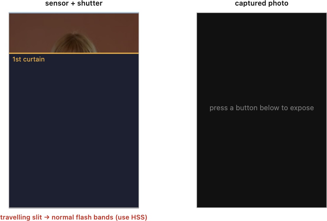
Flash sync speed. This is the moment to pin down a term the last paragraphs kept circling: the flash sync speed is the fastest shutter speed at which the entire frame is open at one instant. A focal-plane shutter only ever fully uncovers the sensor for exposures longer than this — typically around 1/200–1/250 s; push to a faster speed and the second curtain begins closing before the first finishes opening, so the frame is swept by a traveling slit rather than bared all at once. A flash discharges in well under a millisecond — far briefer than the slit's traverse — so above the sync speed it lights only the strip the slit happens to expose, leaving the rest dark: the dreaded partial-flash band. At or below the sync speed the whole frame is open together when the flash fires, so it exposes evenly. (A leaf shutter or a global electronic shutter sidesteps this entirely — opening the whole frame at once, it syncs a flash at any speed; "high-speed sync" fakes the same on a focal-plane shutter by strobing the flash continuously as the slit crawls across, at a steep cost in flash power.) The interactive below makes the curtains, the slit, and the flash timing visible (Figure 2.11.13).
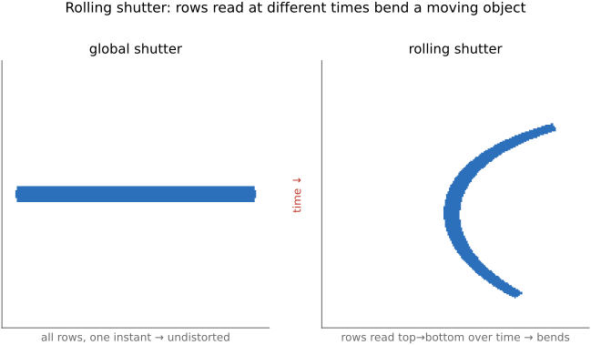
Artificial light adds its own version. Mains-powered lamps and many LED/PWM sources flicker at 100–120 Hz (or faster, when dimmed by pulse-width modulation). Under a rolling shutter, rows captured at different phases of that flicker receive different amounts of light, producing horizontal brightness banding (and color banding if the source's phosphors lag). Cameras fight it with anti-flicker modes that time the readout to the flicker period, by matching the exposure to a multiple of that period, or by using a global shutter outright. And when the artifact cannot be prevented, it can be corrected computationally — by estimating each row's time offset together with the camera and scene motion and warping every row back to a common instant, the subject of the video-stabilization chapter.
2.11.9 A taste of modern sensor tricks⧉
CMOS's per-pixel circuitry enables several useful techniques that recur later.
Dual conversion gain and dual native ISO. A CMOS pixel has a degree of freedom that is invisible in a raw file but shapes its noise: the conversion gain, the voltage swing per collected electron at the readout node, set by the node's capacitance. A smaller capacitance gives a larger voltage per electron — high-conversion-gain (HCG) mode — making the amplifier's noise floor small relative to signal: low read noise, ideal for dark scenes and high ISO. A larger capacitance keeps the well deeper before saturation — low-conversion-gain (LCG) mode — at the cost of higher read noise but with much more highlight headroom. A camera that can switch between the two effectively has two native ISOs (e.g. ISO 800 and ISO 12800), and reading or combining both at once extends the dynamic range of a single exposure (→ Noise, signal-to-noise ratio and dynamic range). This is dual conversion gain (DCG).
Quad-Bayer and high-megapixel phone sensors. Many high-megapixel phone sensors — 48, 50, or 108 MP — use a quad-Bayer mosaic (also marketed as Tetracell or quad CFA) that groups 2×2 same-color photosites under a single color filter. In good light the four sub-pixels are read separately and remosaiced into a standard Bayer pattern, recovering full resolution; in low light they are binned into one larger effective pixel, trading resolution for ~4× better light collection and a lower noise floor (so a 48 MP sensor delivers clean 12 MP low-light output). The 2×2 group can also be exposed at two different times for in-pixel staggered HDR; a 3×3 variant, the Nonacell, bins nine cells.
It is worth being precise about where the binning gain comes from, because it is not free resolution. Combining the four same-color sub-pixels in low-res mode can be done two ways: charge-domain binning, which sums the four charge packets on the shared floating diffusion and reads the total once, or capturing at full resolution and averaging the four reads in software. In the shot-noise-limited (bright) regime the two are essentially identical — both collect the same $4S$ photons over the $2\times2$ area, so $\mathrm{SNR}=\sqrt{4S}$, a clean $2\times$ ($+6$ dB) over a single sub-pixel either way; the read penalty is invisible. The difference shows in the read-noise-limited (low-light) regime: charge binning pays the read noise $\sigma_r$ once for the combined packet, whereas averaging four separate reads pays it four times and then averages, leaving $\sqrt{(S+\sigma_r^2)/(S+\tfrac14\sigma_r^2)}\to 2\times$ ($+6$ dB) more noise in the dark. Concretely, at $S=1\,e^-$ and $\sigma_r=2\,e^-$ per sub-pixel, charge binning gives $\mathrm{SNR}\approx1.4$ against $\approx0.9$ for digital averaging — about $+4$ dB, climbing toward the full $+6$ dB asymptote as the scene darkens. (Beware the "$+12$ dB / $4\times$" figure quoted elsewhere: that compares charge binning to a single un-binned read, not to the averaged full-res image — see the noise chapter.) So the quad sensor is a genuine mode switch: bin in charge for low-light SNR, or read full-res and pay a small SNR price for resolution — you do not get both at once. These sensors need an extra front-end remosaic step that converts the 2×2 (or 3×3) groups into a conventional Bayer mosaic before demosaicking (→ Demosaicking).
Dual-pixel and quad-pixel autofocus. The microlens over a photosite can be shared across two (dual-pixel) or four (quad-pixel, 2×2 on-chip lens) sub-photodiodes, each seeing a different half or quadrant of the lens's exit pupil. Because the two pupil halves form slightly shifted images — exactly a stereo pair — the difference between the sub-diode signals carries a phase proportional to defocus: phase-detection autofocus (PDAF) at every pixel, with no dedicated AF sensor. For the final image the sub-diodes are simply summed, so no light is lost; a quad-pixel (2×2 OCL) arrangement adds sensitivity to both horizontal and vertical phase. The optics and focusing algorithm are in Autofocus.
LOFIC — extending dynamic range in a single exposure. Dual conversion gain, above, widens dynamic range at the dark end by reading the same charge through a quieter amplifier. A lateral overflow integration capacitor (LOFIC) widens it at the bright end, by refusing to throw the bright charge away. Each pixel gets a second charge reservoir beside the photodiode; as the photodiode approaches saturation, the surplus electrons that an ordinary pixel would simply clip instead overflow into the capacitor, which integrates them. At readout the pixel is sampled several ways — a high-gain read for the shadows and the overflow capacitor for the highlights — and merged into one value, so the effective full well swells into the millions of electrons and the single-exposure dynamic range exceeds 100 dB, around sixteen stops, with no bracketing. Because it is genuinely one exposure, it sidesteps the ghosting of multi-shot HDR and the flickering-LED artifacts that plague short sub-exposures — which is why LOFIC took hold first in automotive sensors and, by 2026, in flagship phone sensors such as Sony's LYT-910 (Akahane et al. 2006). The newest designs stack LOFIC with dual conversion gain, reading three signals from one pixel to cover shadows, midtones, and highlights at once. We return to in-sensor HDR, alongside burst HDR, in the multiple-exposure part.
Nano-prism — collecting color without throwing light away. Every Bayer pixel hides a quiet extravagance: its color filter works by absorption, so a "red" pixel discards the green and blue light that strikes it — roughly two-thirds of every photon thrown away, a waste a sub-micron pixel can ill afford. A color router (also called a color splitter or nano-prism) refuses that loss. In place of the absorptive filter it puts an inverse-designed nanostructure — a per-pixel dispersive prism — that redirects each wavelength toward a different neighboring photodiode instead of absorbing it, lifting optical efficiency from the filter's ~33% ceiling toward 80% and beyond (Nishiwaki et al. 2013; Zou et al. 2022). A subtle consequence is that, because the structure scatters one point's red, green, and blue components onto different neighbors, it spreads each point's light across a small neighborhood — formally a mild optical low-pass, a built-in cousin of the anti-aliasing filter a mosaic sensor would otherwise need (we develop this color-multiplexing reading in the colour chapter). The same spreading, pushed too far, becomes resolution-killing inter-pixel crosstalk, so the engineering battle is to separate color cleanly without smearing the picture. The first shipping cousin, Samsung's "Nanoprism," takes the gentler step of replacing only the microlens to steer light into the filters it keeps.
Event sensors. An event sensor (or dynamic-vision sensor) abandons the frame entirely. Each pixel watches the logarithm of the light falling on it and, the moment that value rises or falls by a set threshold, emits a single timestamped event — a tiny message saying "this pixel just got brighter (or darker), now." There is no shutter, no exposure, no synchronized readout: static parts of the scene stay silent while moving edges spray out a sparse stream of events with microsecond timing. The payoffs are dynamic range beyond 120 dB, latency near a microsecond, no motion blur, and milliwatt power — at the cost of producing no ordinary picture at all, since the sensor reports change, not absolute brightness. That trade makes it nearly useless for taking photographs and superb for everything photographs are bad at: high-speed robotics, visual odometry and SLAM, automotive perception, and always-on eye tracking, often paired with a conventional sensor that supplies the appearance the events lack. First built as a 128×128 "silicon retina" by Lichtsteiner, Posch and Delbrück in 2008 (Lichtsteiner et al. 2008), event sensors are now sold by iniVation and Prophesee, the latter in a stacked HD sensor co-developed with Sony.
The rest of the menagerie — stacked sensors and single-photon avalanche diodes — waits in the Advanced part. (The off-axis cos⁴ natural vignetting met in the previous chapter is a related geometry effect, not a sensor trick.)
2.11.10 The impact of sensor size⧉
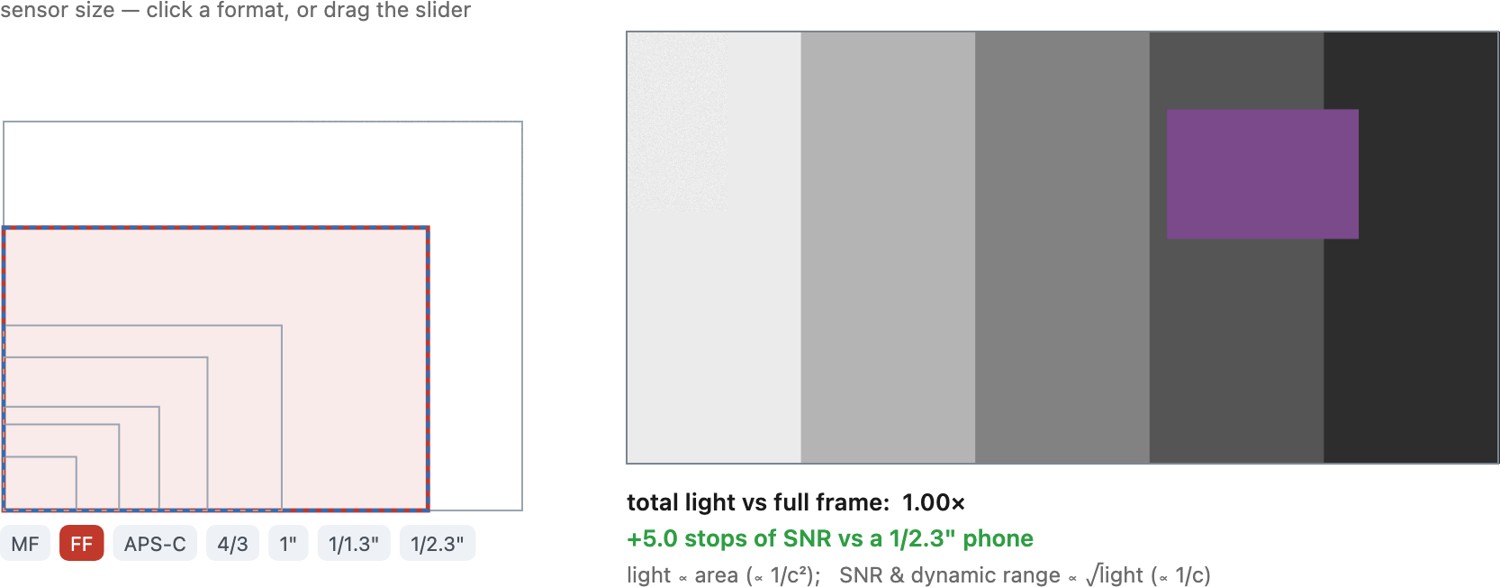
Sensor size is the quiet variable behind half the trade-offs in this book, so it is worth gathering its consequences in one place. The headline number is the crop factor — the ratio of the full-frame diagonal ($43.3$ mm) to the sensor's own diagonal. Full frame is $1\times$ by definition; APS-C is about $1.5\times$, Micro Four Thirds $2\times$, a 1-inch compact $2.7\times$, and a phone's main sensor roughly $7\times$ (smaller still for its ultrawide and tele modules). Almost everything below scales with that one factor.
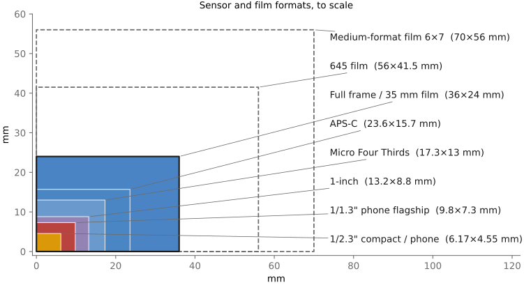
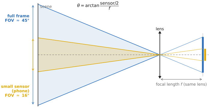
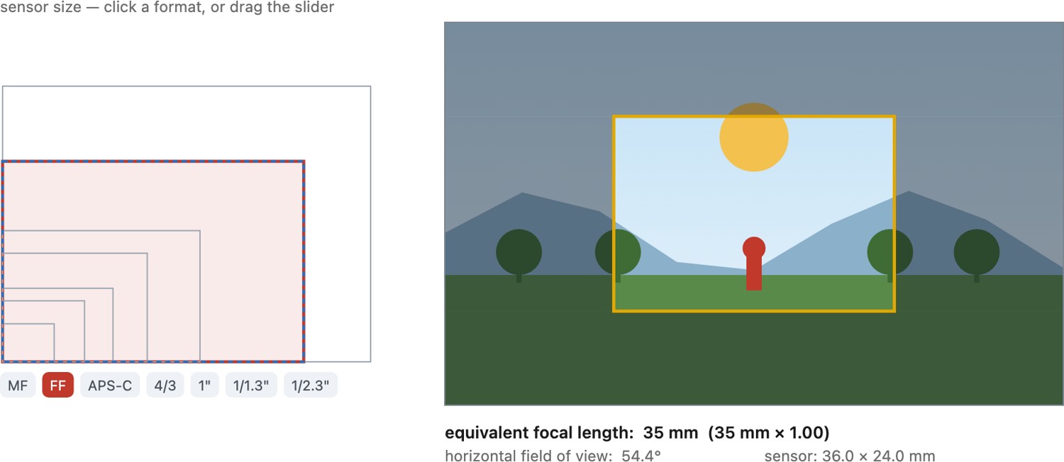
Field of view. A focal length frames differently on every sensor, because field of view depends on sensor size (L2.21, L2.26): the same lens is wide on a big sensor and telephoto on a small one. This is why focal lengths are quoted as a 35 mm equivalent $=$ actual focal length $\times$ crop factor (a phone's ~6 mm lens frames like ~26 mm). The flip side is "reach": a crop body turns a 300 mm lens into the framing of a 450 mm for free — handy for wildlife and sport, at the cost of the wide end.
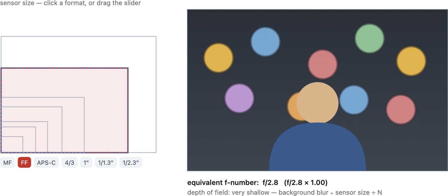
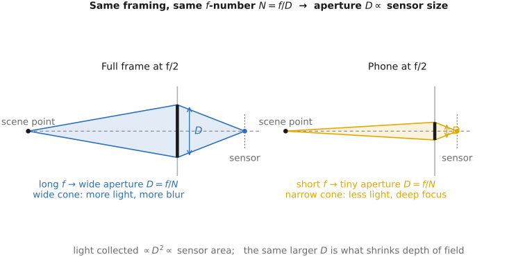
Depth of field. Shrinking the sensor deepens depth of field and shrinks the background blur in proportion (L2.37): at fixed framing and f-number the out-of-focus blur tracks the physical aperture diameter, which scales with the sensor (the ray geometry is in Figure 2.11.20, below). Small sensors therefore give near-universal focus — convenient for snapshots, fatal for bokeh — which is exactly why phones must synthesize shallow depth of field (portrait mode, a later chapter). Equivalently, a phone at $f/1.8$ has the depth of field of full frame at $\approx f/12$.
Light gathering — the real reason big sensors look better. At equal framing and equal f-number, a larger sensor collects more total light, because its aperture is physically larger (same $N=f/D$, but $f$, and hence $D$, are bigger). More photons means a higher signal-to-noise ratio (L2.42) and more dynamic range — this, not pixel count, is why a full-frame photo looks cleaner than a phone photo of the same scene. The advantage is the total sensor area, almost independent of how finely that area is diced into pixels.
What happens as pixels shrink in $x$ and $y$. Scale a sensor (or a pixel) down in the image plane and the photodiode shrinks with it, with two consequences. First, the full-well capacity — the most electrons a pixel can hold before it saturates — scales roughly with photosite area, so a smaller pixel clips its highlights sooner and carries less dynamic range. Second, the depth of the silicon does not shrink in step: it is set by how deep red light penetrates silicon (a few microns, regardless of pixel width), so very small pixels become awkward tall-and-thin wells with more cross-talk between neighbors and harder microlens focusing — part of why sub-micron pixels need back-side illumination and deep-trench isolation to work at all.
What else sensor size touches — the easy-to-forget list: diffraction (a smaller pixel meets the lens's Airy-disk limit sooner, so past a point more megapixels resolve nothing, and the diffraction-limited aperture arrives at a wider f-stop on a small sensor); lens size, weight, and cost (a bigger sensor demands physically bigger glass to cover it — the reason full-frame kits are large and expensive); rolling-shutter skew (a bigger sensor takes longer to read out row by row, so its rolling shutter is worse, all else equal); and manufacturing cost and yield (silicon defects make large sensors disproportionately pricey — a full-frame sensor costs far more than $7\times$ a phone sensor, not $7\times$). Low-light reach, dynamic range, bokeh, lens bulk, and price all trace back to this one dial — which is why "what size is the sensor?" is usually the first question worth asking about any camera.
Almost every camera trade-off scales with the sensor's linear size, captured in the crop factor $c$ (full-frame diagonal $\div$ the sensor's). Three consequences, each with a different scaling:
- Field of view — to match a framing, the equivalent focal length scales linearly, $f_{\text{eq}} = f \times c$ (L2.21, L2.26): a phone's $6$ mm lens frames like $\sim\!26$ mm.
- Depth of field — at fixed framing and f-number the physical aperture diameter, and so the background blur, scale linearly with sensor size, so the equivalent f-number is $N_{\text{eq}} = N \times c$ (L2.37): a phone at $f/1.8$ has full-frame's $f/12$ depth of field. Small sensors give deep, near-universal focus and little bokeh.
- Light and noise — at equal framing and f-number the total light collected scales with sensor area ($\propto c^{2}$), so the photon count does too; photon-noise-limited SNR and dynamic range then scale with the linear dimension ($\sqrt{\text{area}}$, $\propto 1/c$) (L2.42). This total-light advantage, not pixel count, is why a big sensor looks cleaner.
So the bookkeeping is: equivalent focal length and equivalent f-number are linear in sensor size; total light gathered is quadratic (its area); the SNR and dynamic-range benefit go as the linear dimension (the square root of area). One dial, three different exponents.
2.11.11 How far sensors have come⧉
All of this engineering shows up as steady, measurable progress on the three axes that matter — resolution, dynamic range, and low-light — and the most striking landmark is the one from the history of photography: digital sensors caught and then passed 35 mm film on each axis in turn (Figure 2.11.22).
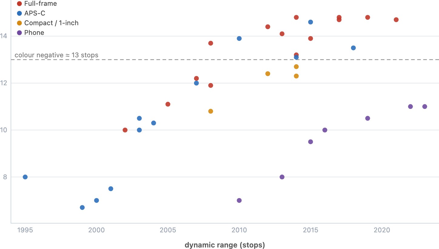
Where the curves are heading now. The recent trend is clear: single-shot dynamic range and low-light performance have largely plateaued. The physics is unforgiving — a pixel of a given area can only collect so many photons before it saturates, and the read-noise floor is already within a fraction of a stop of fundamental limits — so a modern full-frame sensor is only marginally better in a single exposure than one from several years ago. The frontier has moved off the single capture and into computation: the dynamic-range and low-light gains that matter now come from bursts and on-chip HDR, not from a quieter pixel (which is exactly why the rest of this book exists).
Resolution still climbs, but the climb is mostly meaningful on phones: small pixels gain little from more of them on a large sensor (you hit lens resolution and shot noise), whereas a phone uses enormous pixel counts as raw material for binning and computational super-resolution. The headline numbers are startling — mainstream phones now ship 200-megapixel sensors (Samsung's ISOCELL HP-series) — but those pixels exist to be combined: a 200 MP sensor in a dim scene reports a clean ~12.5 MP image by averaging each 16-pixel group, trading nominal resolution for light, and only delivers its full count in bright light. The big-sensor classes, by contrast, have settled into a comfortable 24–60 MP and stopped chasing the number.
The axis that is still improving fast is speed. Stacked (back-illuminated) CMOS bonds the photodiode wafer to a separate logic wafer beneath it, and the newest designs add a layer of on-die DRAM between them. That buffer lets the sensor dump an entire frame off the pixel array almost instantly and read it out from memory at leisure — enabling full-resolution raw at ~30 fps, near-global-shutter readout that tames the rolling-shutter skew above, and blackout-free electronic viewfinders that never drop a frame. Fast readout is also what makes per-pixel on-sensor phase-detection autofocus (the dual- and quad-pixel PDAF described above, and developed in Autofocus) practical at video rates. The deeper stacked-sensor menagerie — and event cameras and single-photon detectors — waits in the Advanced part; the trend to carry forward is that the sensor's recent gains are less about cleaner pixels and more about getting the data off the chip faster so that computation can do the rest.
Recap: big lessons of this chapter
A photosite is at heart a photon counter: each absorbed photon frees a charge carrier — an electron, or equivalently a hole (a missing electron) — and the well accumulates them in direct proportion to the light that arrives. So the raw signal is linear in scene radiance, before any gamma or tone curve. This linearity is not a detail; it is what makes raw arithmetic trustworthy: HDR merging adds exposures, white balance is a per-channel multiply, flat-field correction is a divide, and all three are valid only because the numbers are proportional to light. Display encoding (gamma) deliberately hides this linearity for the eye — so computation should undo it and work in linear light.
Strip away the color filter and a sensor is monochrome at the pixel: each photosite reports a single number, the count of photons it caught — not a color. The three (or more) values that color needs must therefore be multiplexed along some other axis: over space (a color-filter array such as Bayer, paying with resolution and a demosaicking step), over time (sequential color filters, paying with motion robustness — the old color-wheel and many scientific cameras), across multiple sensors (a beam-splitter prism feeding three chips, the 3-CCD video camera, paying with bulk and cost), or over depth (wavelength-dependent absorption in stacked photodiodes, the Foveon, paying with noise). Every color camera is a choice of which axis to spend. The same constraint shapes the eye, whose three cone types sample color over space at the retina (L2.10, L2.13).
Almost every camera trade-off scales with the sensor's linear size, captured in the crop factor $c$ (full-frame diagonal $\div$ the sensor's). Three consequences, each with a different scaling:
- Field of view — to match a framing, the equivalent focal length scales linearly, $f_{\text{eq}} = f \times c$ (L2.21, L2.26): a phone's $6$ mm lens frames like $\sim\!26$ mm.
- Depth of field — at fixed framing and f-number the physical aperture diameter, and so the background blur, scale linearly with sensor size, so the equivalent f-number is $N_{\text{eq}} = N \times c$ (L2.37): a phone at $f/1.8$ has full-frame's $f/12$ depth of field. Small sensors give deep, near-universal focus and little bokeh.
- Light and noise — at equal framing and f-number the total light collected scales with sensor area ($\propto c^{2}$), so the photon count does too; photon-noise-limited SNR and dynamic range then scale with the linear dimension ($\sqrt{\text{area}}$, $\propto 1/c$) (L2.42). This total-light advantage, not pixel count, is why a big sensor looks cleaner.
So the bookkeeping is: equivalent focal length and equivalent f-number are linear in sensor size; total light gathered is quadratic (its area); the SNR and dynamic-range benefit go as the linear dimension (the square root of area). One dial, three different exponents.